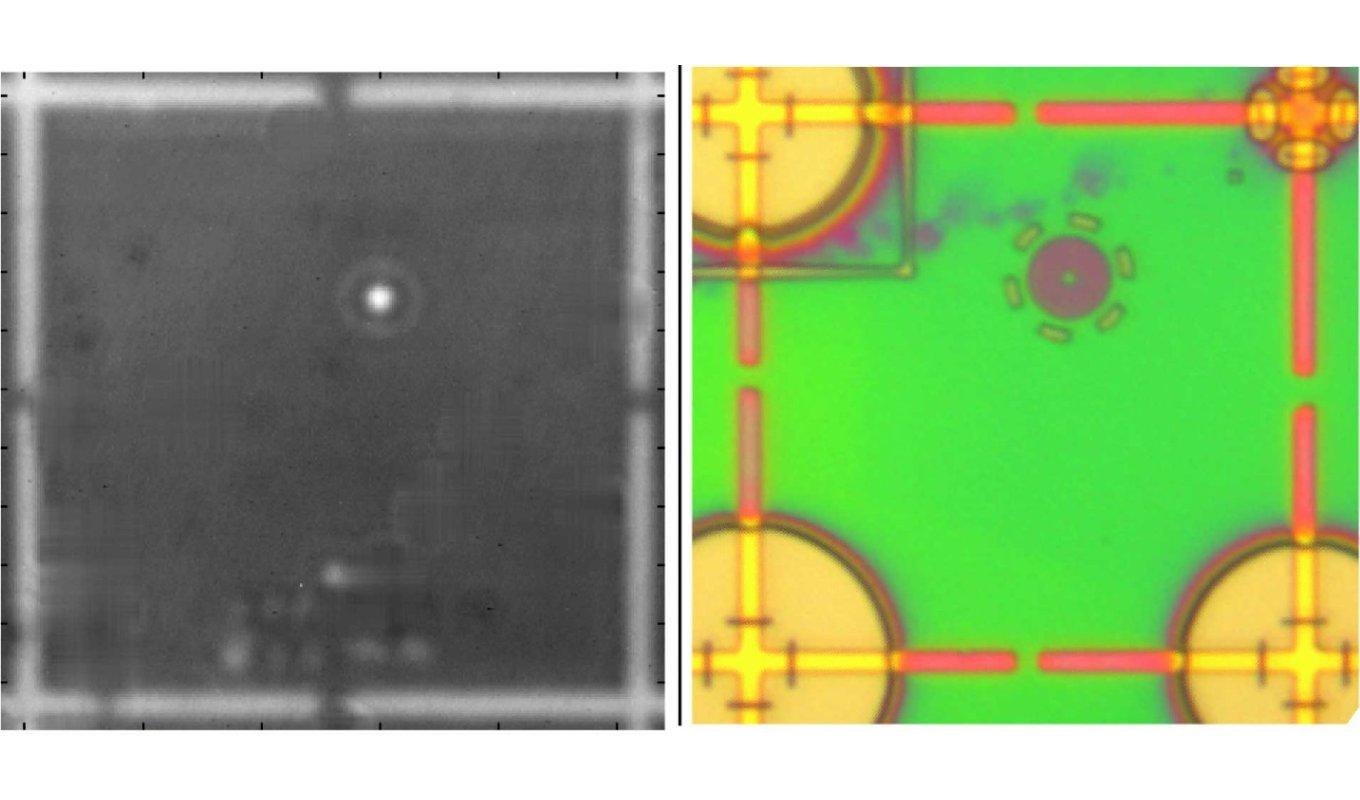
Fluorescence imaging (left) is used to locate a single quantum dot with respect to alignment marks, after which a photonic device (right) is built in the correct location for enhancing the quantum dot properties.
Solid-state quantum emitters such as InAs/GaAs quantum dots are key for realizing high-performance, chip-integrated quantum technologies like single-photon sources and single-photon gates. In most cases, however, this requires they they can be reliably located within the appropriate spatial locations in high quality factor, small mode volume optical cavities. However, the most common way to grow such quantum dots, via epitaxial self-assembly, results in random spatial locations of quantum dots within the plane of the growth wafer. In this article by our colleagues Shunfa Liu and Jin Liu (Sun-Yat Sen University) and Kartik, we review the different nanoscale positioning approaches that have been implemented within the community to enable high-performance quantum photonic structures based on single solid-state quantum emitters.
S. Liu, K. Srinivasan, and J. Liu, "Nanoscale Positioning Approaches for Integrating Single Solid-State Quantum Emitters with Photonic Nanostructures", Laser & Photonics Reviews, 2100223 (2021).